Semiconductor Metrology
Bruker Semiconductor develops, manufactures, markets, and supports metrology solutions for thin films, which are based on novel, rapid, non-contacting and non-destructive X-ray technology. With Bruker’s acquisition of Jordan Valley Semiconductors, a name synonymous with unparalleled worldwide customer service and support, 75% of the world's top 25 semiconductor manufacturers rely on Bruker metrology tools for front-end and back-end applications, including development of their next-generation thin films. Bruker commitment to innovation and technology leadership drives the continued release of new advancements in metrology, and has garnered numerous awards and industry recognition.
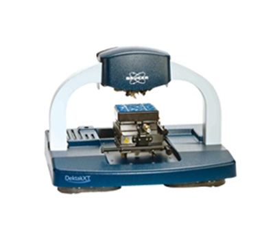
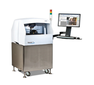
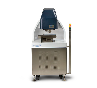
In applications ranging from C-S thin films materials characterization to wafer substrate analysis and defect detection, Bruker’s systems provide simulation analysis and fit. Stylus Profilers,Micro XRF M4 TORNADO measurement types are fully supported, enabling researchers, production engineers, and process developers unparalleled capabilities. Whether you are a semi and C-S fabricator, R&D center or academy, or an industry materials research facility, Bruker has a specifically designed solution for your metrology needs.
Click to learn more product information.
Contact our application team immediately: 021-37018108, info@boyuesh.com
Tel:86-021-37018108
Fax:86-021-57656381
Email:info@boyuesh.com
Address:Room 301, 28 Songjiang Hi-tech park, 518 Xinzhuan Road, Songjiang District, Shanghai